Chapter 8
Frequency Response
Gordon W. Roberts
Department of Electrical & Computer Engineering, McGill University
In this chapter we shall investigate the frequency response behavior of various amplifier circuits using Spice. Among other things, this will enable us to verify the accuracy of the gain and bandwidth expressions derived by a hand analysis.
|
Fig. 8.1: General form of the LTSpice element statement for a voltage or current dependent-source with its gain written as a function of the complex frequency variable. |

|
(a)
(b)
Fig. 8.2: (a) A simple circuit arrangement for investigating transfer function behavior, (b) LTSpice captured schematic with Spice directive.
|
Using LTSpice to create a Bode Plot of Transfer Function T(s)
* * Circuit Description * * input signal V1 IN 0 0V AC 1V 0deg * VCVS with transfer function: * 10s * T(s) = --------------------------- * ( 1+s/10^2 ) ( 1 + s/10^5 ) R1 IN 0 1 R2 OUT 0 1 * E1 OUT 0 IN 0 Laplace={(10*s) / ( (1+s/1e2) * (1+s/1e5) )} * * Analysis Requests * .AC DEC 10 1mHz 100MegHz .backanno .end
Fig. 8.3: The LTSpice generated circuit netlist for the circuit arrangement of Fig. 8.2 including the Laplace transform statement.
|


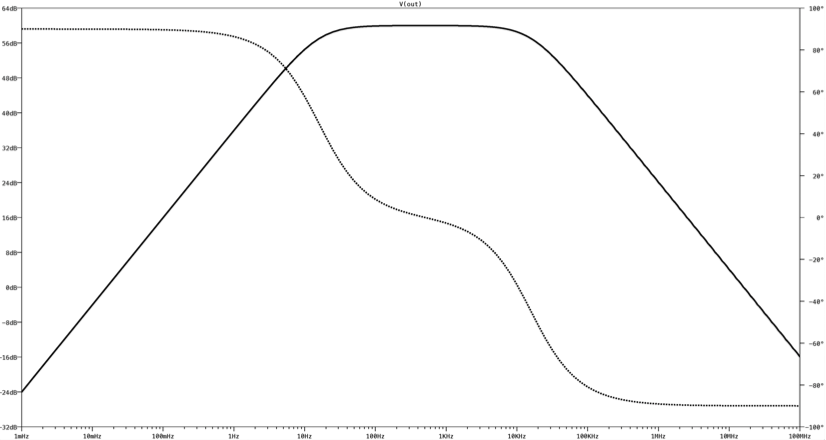
Fig. 8.4: Magnitude and phase response of the transfer function given in Eqn. (8.1) as calculated and plotted by LTSpice.
8.1 Investigating Transfer Function Behavior Using LSpice
A useful feature of LTSpice is the ability to specify the frequency-dependent gain of a current or voltage dependent-source as a Laplace Transform function. Although one could envision many new applications of this feature; here we are mainly concerned with it as a means for investigating transfer-function behavior as a function of frequency.
Specifying the gain of a dependent source as a Laplace transform function is restricted in LTSpice to only the VCVS and VCCS (designated with the letters E and G, respectively). The general form of the element statement used to specify the gain of either one of these controlled sources in terms of the Laplace variable s is illustrated in Fig. 8.1. The first part of this statement, before the keyword Laplace, is identical to that given previously for either the VCVS or VCCS (i.e., element type with a unique name and the nodes the dependent source is connected to). After the keyword Laplace, the variable that the controlled source depends on is specified between braces (e.g., { V(1) } ). An equal sign (=) is necessary to connect the word Laplace and an expression written in terms of the Laplace variable.
Having the ability to specify gain as an arbitrary expression in terms of the Laplace s-variable provides a simple means for investigating transfer-function frequency behavior. Consider the simple circuit in Fig. 8.2. Here a VCVS having a voltage gain expressed in the form of a transfer function T(s) is excited by an input AC voltage source of 1 V of arbitrary frequency. As a result, the voltage appearing across the output port is equal directly to the transfer function, i.e., Vo(s)=T(s). Thus, using the AC analysis command of LTSpice, one can investigate the behavior of the transfer function T(s) for physical frequencies defined by s=jw.
Consider the simple circuit in Fig. 8.2(a). Here a VCVS having a voltage gain expressed in the form of a transfer function T(s) is excited by an input AC voltage source of 1 V of arbitrary frequency. As a result, the voltage appearing across the output port is equal directly to the transfer function, i.e., Vo(s)=T(s). Thus, using the AC analysis command of LTSpice, one can investigate the behavior of the transfer function T(s) for physical frequencies defined by s=jw. Resistors R1 and R2 are included in the circuit of Fig. 8.2(a) to act as a load for the two voltage sources. A warning will be generated in the Spice Error Log file if this is not done but it will still function correctly. The circuit of Fig. 8.2(a) was drawn using the schematic capture feature in LTSpice to produce the schematic drawing shown in Fig. 8.2(b). An .AC analysis command was included in the command window to sweep the frequency in a logarithmic manner from 1 mHz to 100 MHz using 10 points per decade. Here the following Laplace transfer function was described as the value attribute for the E1 voltage source:
(8.1)
As a point of reference, the LTSpice generated circuit netlist is provided in Fig. 8.3. Reviewing this file confirms the Laplace syntax of the VCVS, E1.
The output response of the circuit across frequency is shown graphically in Fig. 8.4. The solid line represents the magnitude response expressed in dBs and corresponds to the vertical scale to the left. The phase response is plotted with a dotted line and corresponds to the scale on the right, expressed in degrees. The magnitude scale on the left can be changed to a linear or logarithmic scale rather than dB scale by moving the mouse over the units of the left scale and clicking the right mouse button. In a similar way, the phase scale can also be altered.
|
(a) |
(b) |
(c) |
|
Fig. 8.5: Dynamic Spice models of the small-signal behavior of: (a) junction diode (b) BJT and (c) MOSFET.
|
||


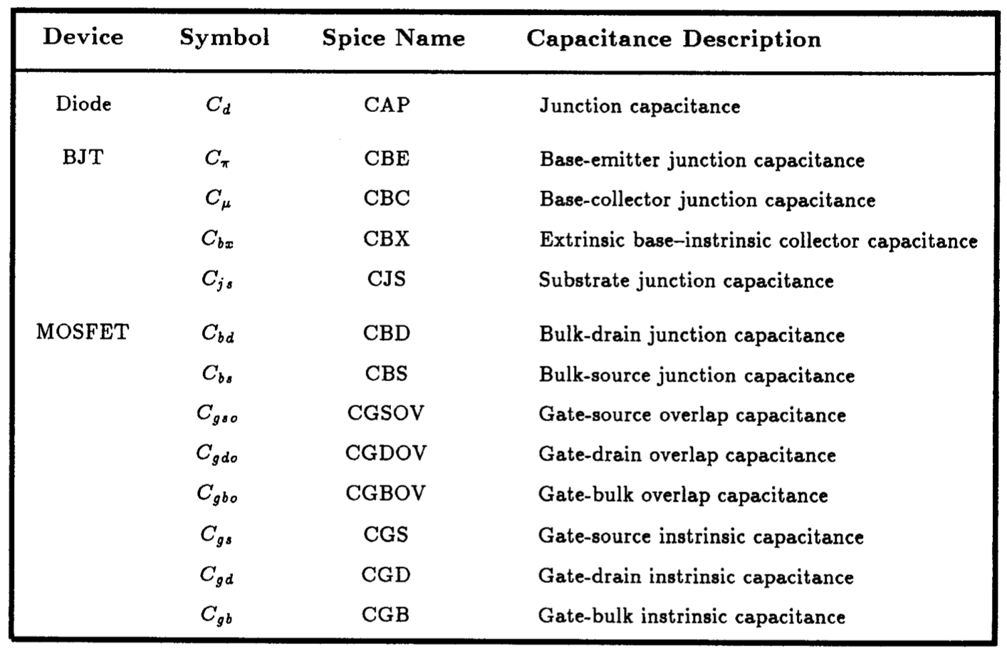
Table 8.1: Capacitances associated with the small-signal models of the diode, BJT and MOSFET shown in Fig. 8.5.
|
Fig. 8.6: One particular bias arrangement for the commercial transistor 2N2222.
|

8.2 Modeling Dynamic Effects in Semiconductor Devices
LTSpice performs frequency domain analysis on diode and transistor circuits in much the same way that one performs this analysis by hand. Each diode or transistor in the circuit is replaced by its small-signal frequency-dependent equivalent circuit, and all DC voltage sources are shorted to ground, and all DC current sources are open circuited. Standard frequency-domain circuit analysis techniques are then applied to the equivalent small-signal circuit to determine the signal levels at various nodes or branches of the circuit.
The small-signal frequency domain model of either a diode or a transistor is similar to the small-signal model of the semiconductor device under static conditions with the exception that capacitors are included to account for the frequency effects. In Fig. 8.5 we illustrate the small-signal dynamic models of the semiconductor junction diode, the BJT, and the MOSFET as generally used by LTSpice. The BJT small-signal model applies equally well to both npn and pnp devices. Similarly, the FET model applies to both n-channel and p-channel devices. Except for the additional capacitors included in these models, they are identical to those introduced in previous chapters. Table 8.1 provides a cross-reference of the names of each capacitor in each of these models used here with those used by LTSpice.
To gain insight into circuit frequency-domain behavior, it is sometimes useful to know the value of the parameters of the small-signal model used by LTSpice in AC analysis. This information is sent to the Spice Error Log file when an .OP (operating point) command is included as a Spice directive. Consider, for example, that we are biasing of the commercial 2N2222 transistor with a 10 𝜇A base current and a collector-emitter voltage of 5 V, as illustrated in Fig. 8.6 using the LTSpice schematic capture. On completion of the .OP analysis, the following parameters pertaining to the small-signal BJT model are found:
|
Semiconductor Device Operating Points:
--- Bipolar Transistors ---
Name: q1 Model: 2n2222 Ib: 1.00e-05 Ic: 2.07e-03 Vbe: 6.74e-01 Vbc: -4.33e+00 Vce: 5.00e+00 BetaDC: 2.07e+02 Gm: 7.96e-02 Rpi: 2.59e+03 Rx: 1.00e+01 Ro: 5.03e+04 Cbe: 7.15e-11 Cbc: 4.26e-12 Cjs: 0.00e+00 BetaAC: 2.06e+02 Cbx: 0.00e+00 Ft: 1.67e+08
Operating Bias Point Solution:
V(c) 5 voltage V(n001) 0.673565 voltage Ic(Q1) 0.00207279 device_current Ib(Q1) 1e-05 device_current Ie(Q1) -0.00208279 device_current I(Ib) 1e-05 device_current I(Vce) -0.00207279 device_current
|
Here we see a list describing the transistor small-signal model parameters and the circuit’s DC operating point. Most parameters of the small-signal model should be self-evident from the above list. Capacitors CBE and CBC are equivalent to capacitances Cp and Cu, respectively, of the usual hybrid-pi model. Several capacitances of this particular transistor, specifically CBX and CJS, are zero because they represent capacitive coupling to the substrate of the device. Since the 2N2222 is a discrete transistor, constructed from a sandwich of three separate layers of semiconductor material, it has no substrate layer. As a result, LTSpice simply assumes that these substrate capacitances do not exist and are set equal to zero.
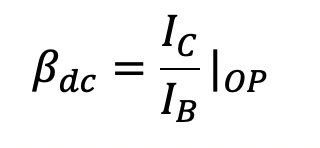
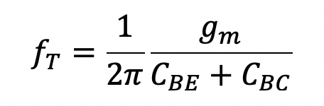
In addition to printing the hybrid-pi model parameters, LTSpice also computes and prints the values βdc, βac and fT, which are related to the transistor's operating point according to the following equations:
(8.2)
(8.3)
and
(8.4)
For this particular case, this transistor has a DC current gain of 207 and an AC current gain of 206. It is important to note that in general these values are different, but more importantly, that they can be quite different than the value of βF specified on the model statement used to describe the device in the model statement. The model statement for the 2N2222 is shown below:
|
.model 2N2222 NPN (IS=1E-14 VAF=100 BF=200 IKF=0.3 XTB=1.5 BR=3 CJC=8E-12 CJE=25E-12 TR=100E-9 TF=400E-12 + ITF=1 VTF=2 XTF=3 RB=10 RC=.3 RE=.2 Vceo=30 Icrating=800m mfg=NXP)
|
As is evident, BF=200, which is different from βDC or βAC. This arises because the dependence of the transistor current gain on collector current is captured by the Spice model for the 2N2222.
Also, one can see that the unity-gain bandwidth fT for this transistor was computed by LTSpice to be about 167 MHz. There is no corresponding parameter used in the Spice model.
Similar ideas extend to JFETs, MOSFETs, MESFETs and junction diodes.
|
(a)
(b)
Fig. 8.7: (a) A capacitive coupled common-source JFET amplifier. (b) LTSpice captured schematic with AC analysis directive.
|


|
Fig. 8.8: The low-frequency magnitude response of the capacitively coupled common-source JFET amplifier shown in Fig. 8.7. Three straight lines having slopes of +40 dB/dec, +20 dB/dec, and 0 dB/dec, are superimposed on the magnitude response of the amplifier to illustrate the approximate locations of the different break frequencies.
|

8.3 The Low-Frequency Response of the Common-Source JFET Amplifier
In this section we shall investigate the low-frequency response of the classical common-source JFET amplifier shown in Fig. 8.7(a). The component values for this particular circuit were selected such that the low-frequency response of this amplifier is dominated by a pole at 100 Hz and that the nearest pole or zero will be at least a decade away at a lower frequency. Using LTSpice schematic capture shown I Fig. 8.7(b), we shall verify whether this is indeed the case. The device parameters of the n-channel JFET are assumed to be as follows: Vt0=-2 V, β=2 mA/V2 and lambda=0 V-1. The amplifier input is excited by a 1 V AC input signal and an AC frequency sweep command is included in order to compute the small-signal frequency response of the amplifier. A logarithmic sweep of 10 points per decade varies the input frequency of excitation beginning at 1 Hz and ending at 1 kHz. A corresponding plot command as the output request command will then produce a plot of the magnitude of the amplifier output voltage as a function of frequency. Also included in this input file is an .OP command. The results of this analysis are used to verify that the amplifier is operating correctly in its linear region (i.e., J1 is in pinch-off). This is left for the reader to confirm.
The magnitude frequency response behavior of the JFET amplifier, as calculated by LTSpice, is shown in Fig. 8.8. The midband voltage gain is found to be +20.57 dB, and the 3-dB frequency is located very near to 100 Hz. The magnitude response of the JFET amplifier shown in Fig. 8.9 does not have a simple one-pole response - instead, the magnitude response increases at a rate of +40 dB/dec for low frequencies, much like a two-pole response. We see that the magnitude response increases at this rate until about 10 Hz when the rate of rise in magnitude decreases to +20 dB/dec. This continues until 100 Hz when the magnitude levels off at a constant +20.57 dB for increasing frequencies. This is clarified by the addition of the three straight lines seen superimposed on the graph containing the magnitude response of the amplifier in Fig. 8.8. It appears as though the dominant pole is located at about 100 Hz and the nondominant pole is located at 10 Hz. The effect of the zero (putting aside the two zeros at DC) is nullified by the presence of another pole located quite close to it. We thus confirm that the dominant pole and the next closest pole or zero are approximately one decade apart.
|
(a)
|
Fig. 8.10: LTSpice captured schematic representing the two circuits of Fig. 8.9 with AC analysis directive indicated.
|
|
(b)
Fig. 8.9: (a) The small-signal high-frequency equivalent circuit of a common-source FET amplifier (b) Simplified circuit using the Miller approximation to eliminate the bridging capacitor Cgd. |


|
Fig. 8.11: Comparing the high-frequency response behavior (magnitude and phase) of the circuit shown in Fig. 8.10(a) with the circuit shown in part (b) of the same figure simplified using Miller's theorem.
|

8.4 The High Frequency Analysis of a Common-Source Amplifier
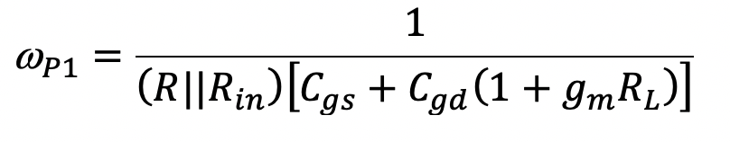
Miller's theorem is commonly used to simplify the task of analyzing electronic circuits. It is especially useful when estimating the upper 3 dB bandwidth of a common-source or common-emitter amplifier. Consider the small-signal equivalent circuit of a common-source amplifier, shown in Fig. 8.9(a). This circuit would be representative of the small-signal equivalent circuit derived for the common-source amplifier shown previously in Fig. 8.8. Calculating the upper 3 dB bandwidth of this amplifier is complicated by the presence of bridging capacitor Cgd. Through the application of Miller's theorem, and assuming that the voltage gain from the gate to drain of J1 is known (i.e., vo » -gmRLvgs), we can approximate the low-frequency behavior of the circuit shown in Fig. 8.9(a) with that shown in part (b). Clearly, the transfer function vo/vi of the circuit shown in Fig. 8.9(b) is dominated by a single pole located at frequency wp1 given by,
(8.5)
With the aid of LTSpice, and some numerical values, we would like to investigate the validity of this Miller approximation by comparing the frequency response behavior of each circuit shown in Fig. 8.9, and determine whether the estimate of 3 dB bandwidth is in agreement with that computed directly from the original circuit. Assuming the same component values as used in the previous example of the last section (with some simplifications), i.e., R=100 kΩ, Rin=420 kΩ, RL=3.33 kΩ, Cgs=1 pF, Cgd=1 pF and gm=4 mA/V, the schematic capture used to describe these two circuits to LTSpice can be seen in Fig. 8.10. Here two circuit description are contained in the same LTSpice schematic capture window concatenated together in order to compare their respective outputs using the cursor facility of LTSpice. A frequency response calculation beginning at 1 kHz and ending at 100 GHz is to be performed using a logarithmic sweep of 10 points per decade. Such a wide frequency sweep is necessary to capture all of the interesting frequency domain behavior of the two circuits shown in Fig. 8.9.
On completion of LTSpice, we display the magnitude and phase of the output voltage Vo as a function of frequency for the two circuits shown in Fig. 8.11. This, of course, corresponds directly to the transfer functions of the two circuits because a 1 V AC input is applied to each circuit. As is evident from the magnitude response of the two circuits, both have very similar behavior for frequencies below 100 MHz. Above this frequency, the phase characteristics of the actual circuit undergoes a change of 180 degrees, but its magnitude behavior remains relatively unchanged. Detailed analysis reveals the presence of a right-half-plane zero located near a second nondominant pole around 500 MHz, thus nullifying the effect of the second (nondominant) pole on the magnitude characteristics while adding to the overall phase. The 3-dB frequency for both networks is located at exactly the same location, at approximately 130 kHz. Interestingly enough, this frequency agrees quite closely with the value obtained through Eqn. (8.5) at 128.6 kHz. Thus, the Miller approximation appears to be quite accurate in estimating the upper 3 dB frequency of this amplifier.
|
(a)
|
|
|
(b)
Fig. 8.12: Two high-frequency amplifier configurations: (a) common-emitter (b) cascode.
|
Table 8.2: General expressions for estimating the midband gain (AM) and 3 dB frequencies (wL and wH) of the common-emitter and cascode amplifiers.
|


|
Fig. 8.13: LTSpice captured schematic of the common-emitter and cascode amplifiers of Fig. 8.12.
|

|
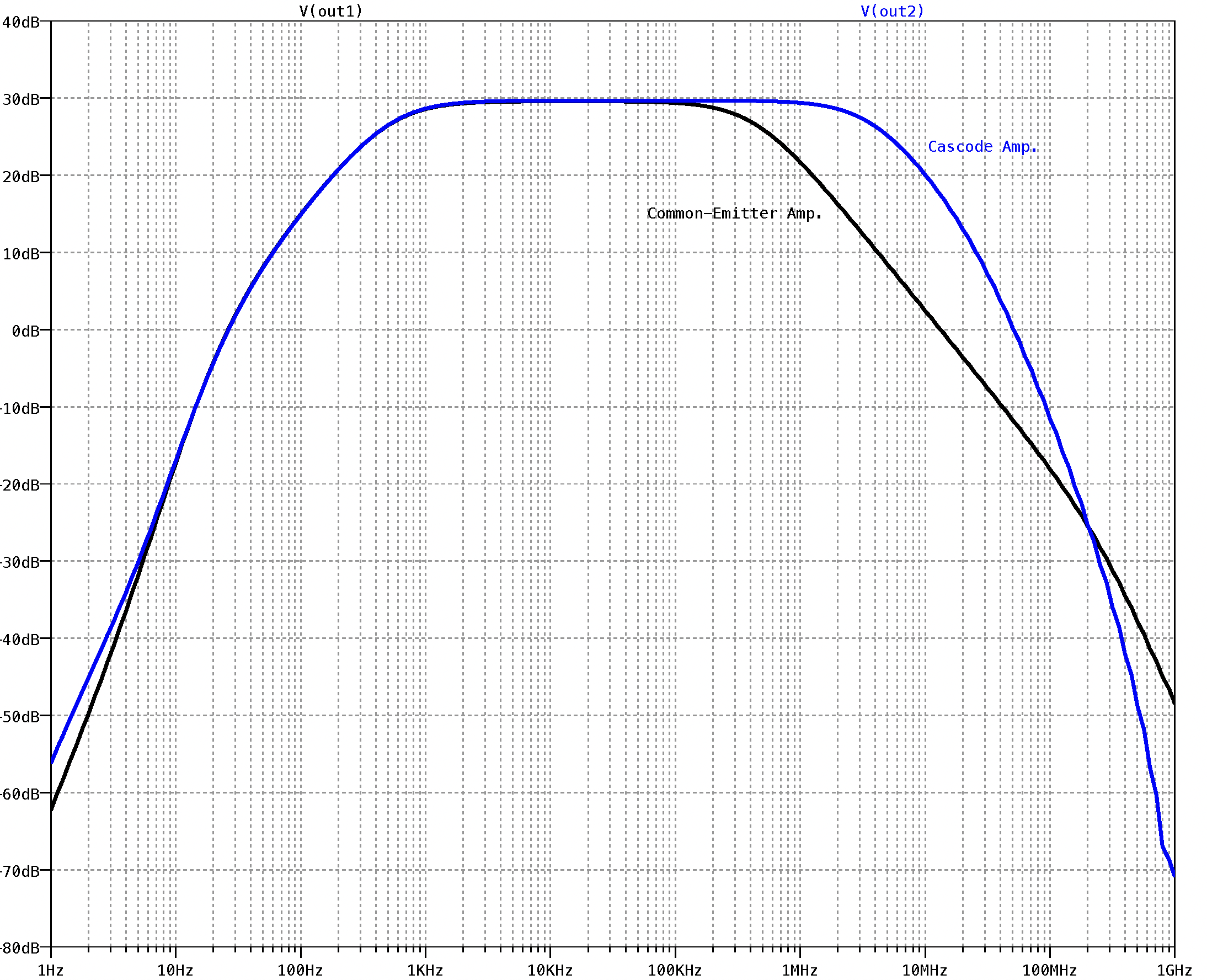
Fig. 8.14: A comparison of the frequency response of the two amplifier configurations presented in Fig. 8.13.
|
|
Table 8.3: The midband gain and 3 dB frequencies of the common-emitter and cascode amplifiers as computed by hand and as obtained by exact analysis using LTSpice. The rightmost column presents the relative error (in percent) between the value predicted by hand and Spice.
|

8.5 High-Frequency Response Comparison of The Common-Emitter and Cascode Amplifiers
Figure 8.12 illustrates two different styles of high-frequency amplifier configurations; these being, the common-emitter amplifier and the cascode amplifier. In the following we would like to use LTSpice to analyze the high-frequency operation of these two amplifier configurations, confirm the formulas used to estimate amplifier midband gain and 3 dB bandwidth, and in the process, determine which amplifier configuration is more suited for high-frequency operation. For a realistic comparison, we shall use identical transistors in both amplifiers and model them after the commercially available 2N3904 npn transistor (available in the LTSpice built-in library). Furthermore, we note that fair comparisons can be made between the different amplifiers because the load and source resistances are identical in each case.
Figures 8.13 illustrate the LTSpice schematic circuit capture for these two amplifiers. Both amplifiers are included in one command window to allow comparison of both. Here an operating point (.OP) command and an AC analysis (.AC) command are included as the Spice directives. The .OP command is deactivated at first. The operating point command is included in order to obtain the small-signal model parameters for the 2N3904 transistor. In Table 8.2 we summarize the hand-analysis formulas that apply to these two amplifiers. The predictions made by these formulas will be compared to those generated by LTSpice.
The results of the AC analysis are displayed in Fig. 8.14. Here we see the magnitude response of the two amplifiers. As is evident, both amplifiers have very similar low frequency response, but quite different high frequency behavior. Each amplifier has a lower 3 dB frequency of about 436 Hz and a midband gain of approximately 30 dB. In the case of the common-emitter amplifier, the upper 3 dB frequency is limited to 441 kHz. This is in contrast to the cascode amplifier which has an upper 3 dB frequency of more than 3.8 MHz. Clearly then, the cascode amplifier has a 3-dB bandwidth more than 10 times that of the common-emitter amplifier and would therefore be the preferred choice as a wideband amplifier.
To illustrate the accuracy in our hand analysis, we present in Table 8.3 a comparison of the midband gain and 3 dB frequencies of each amplifier as calculated using the equations presented in Table 8.2 and as computed by exact analysis using LTSpice. In the hand calculations, we make use of the small-signal model parameters generated by LTSpice for each transistor of each amplifier. The actual operating point information found in the LTSpice output file is as follows:
|
Semiconductor Device Operating Points:
--- Bipolar Transistors ---
Name: q3 q2 q1 Model: 2n3904 2n3904 2n3904 Ib: 3.23e-06 3.30e-06 3.30e-06 Ic: 9.97e-04 1.00e-03 1.01e-03 Vbe: 6.55e-01 6.55e-01 6.55e-01 Vbc: -3.06e+00 -1.34e+00 -1.96e+00 Vce: 3.71e+00 2.00e+00 2.62e+00 BetaDC: 3.08e+02 3.03e+02 3.05e+02 Gm: 3.85e-02 3.86e-02 3.89e-02 Rpi: 7.99e+03 7.83e+03 7.82e+03 Rx: 2.00e+01 2.00e+01 2.00e+01 Ro: 1.03e+05 1.01e+05 1.01e+05 Cbe: 2.60e-11 2.61e-11 2.62e-11 Cbc: 2.34e-12 2.85e-12 2.62e-12 Cjs: 0.00e+00 0.00e+00 0.00e+00 BetaAC: 3.08e+02 3.02e+02 3.04e+02 Cbx: 0.00e+00 0.00e+00 0.00e+00 Ft: 2.16e+08 2.13e+08 2.15e+08
|
To illustrate the accuracy of the expressions found in Table 8.2, we created a third column in Table 8.3 which expresses the relative error in the hand calculation as compared to the results computed by LTSpice. As is clearly evident, hand analysis provides very reasonable estimates of the amplifiers midband gain and 3 dB frequencies, with at most, a 28 per-cent error.
Although the above hand analysis resulted in very reasonable numbers when compare with those obtained directly by LTSpice, it should be pointed out here that these results should not suggest to the reader that LTSpice is not really necessary to compute the frequency response behavior of circuits. In fact, LTSpice is useful in several ways: (1) LTSpice can provide more accurate results than that which is possible by hand analysis; (2) LTSpice provides a very easy way of investigating component trade-offs in a design by allowing the designer to simply change component values and observe the effect on the frequency response; (3) Unlike hand analysis, LTSpice is not limited by the complexity of the circuit. However, one has to be sensible in the application of LTSpice, otherwise one might end up swamped in a morass of results that are difficult to interpret or derive any design insight from.
|
Fig. 8.15: The common-collector common-emitter cascade amplifier configuration.
|
Table 8.4: General expressions for estimating the midband gain (Am) and 3 dB frequencies wL and wH of the common-collector common-emitter cascode amplifier.
|


|
Fig. 8.16: LTSpice captured schematic of the common-emitter-common-collector cascade of Fig. 8.15.
|

|
Fig. 8.17: The magnitude response of the common-collector common-emitter cascade shown in Fig. 8.16 as computed by LTSpice.
|

|
Table 8.5: The midband gain and 3 dB frequencies of the common-collector common-emitter cascade amplifier as computed by hand and exact analysis using LTSpice. The rightmost column presents the relative error (in percent) between the value predicted by hand and LTSpice.
|

8.6 High-Frequency Response of the CC-CE Amplifier
Another important high frequency amplifier configuration is the common-collector common-emitter (CC-CE) cascade. An example of this type of amplifier is shown in Fig. 8.15. Here, a common-collector stage isolates the source resistance RS from the Miller capacitance of the common-emitter stage, thus extending the high frequency operation. In the following we would like to use LTSpice to analyze the high-frequency operation of this amplifier configuration and investigate the validity of the formulae used to estimate the amplifier's midband gain and 3 dB frequencies. For easy reference, we summarize these expressions in Table 8.4.
The schematic captured by LTSpice for this amplifier is shown in Fig. 8.16. Each transistor is modeled after the commercially available 2N3904 transistor. Both a DC operating point and AC analysis command are indicated.
The frequency response of the CC-CE amplifier as calculated by LTSpice is shown in Fig. 8.17. Using the cursor facility of the waveform editor of LTSpice, we can read off this graph and find that the midband gain is 43.7 dB or 153.5 V/V. In addition, we also find that the lower 3 dB frequency of this amplifier is 292 Hz and its upper 3 dB frequency is 6.6 MHz. Also evident in this magnitude plot is signs of high frequency resonance (i.e., magnitude peaking). As we shall see when we compare our hand analysis results with those obtained using LTSpice, this resonant peaking extends somewhat the upper 3 dB frequency of this amplifier which is not accounted for in our hand analysis equations. The gain-bandwidth product of this amplifier is approximately 1010 MHz, which is the largest of any of the amplifiers that we have seen so far (e.g., The CE and Cascode stage presented in the last section had gain-bandwidth product of 13.3 MHz and 115 MHz, respectively.)
To investigate the accuracy of the expressions listed in Table 8.4 for the CC-CE amplifier stage, we compare the midband gain and 3 dB frequencies as calculated by hand with those obtained using LTSpice in Table 8.5. For the hand calculations, we made use of the small-signal model parameters for Q1 and Q2 as generated by LTSpice using the .OP analysis command and repeated here below:
|
Semiconductor Device Operating Points:
--- Bipolar Transistors --- Name: q2 q1 Model: 2n3904 2n3904 Ib: 7.60e-06 6.36e-06 Ic: 2.31e-03 2.10e-03 Vbe: 6.77e-01 6.72e-01 Vbc: -1.76e+00 -1.03e+01 Vce: 2.44e+00 1.10e+01 BetaDC: 3.04e+02 3.29e+02 Gm: 8.90e-02 8.11e-02 Rpi: 3.39e+03 4.04e+03 Rx: 2.00e+01 2.00e+01 Ro: 4.39e+04 5.23e+04 Cbe: 4.39e-11 4.11e-11 Cbc: 2.68e-12 1.65e-12 Cjs: 0.00e+00 0.00e+00 BetaAC: 3.02e+02 3.28e+02 Cbx: 0.00e+00 0.00e+00 Ft: 3.04e+08 3.02e+08
|
As can been seen from Table 8.5, the value of the midband gain calculated by hand is in very good agreement with that obtained from LTSpice (-1.4% error). Both the lower and upper 3 dB frequencies (fL and fH) computed by the hand analysis differ from the results computed by LTSpice with an absolute error of no more than 11 per-cent. In the case of the upper 3 dB frequency, we attribute most of this error to the high-frequency magnitude peaking that seems to extend the high-frequency operation of the CC-CE amplifier stage. The formula derived for the upper 3 dB frequency and used in the hand analysis above assumes that all circuit poles are real; magnitude peaking is an indication that some of the poles are complex.
|
(a)
|
(b)
|
(c)
|
|
Fig. 8.18: Various differential amplifier configurations with single-ended excitation (a) differential amplifier (b) differential amplifier including emitter resistance (c) differential amplifier in common-collector common-base configuration.
|
||


|
Fig. 8.19: LTSpice captured schematic of the three differential amplifier configurations shown in Fig. 8.18. Two Spice directives are listed: dc and ac operating point analysis.
|

|
Fig. 8.20: A comparison of the high-frequency magnitude response of the three differential amplifier configurations presented in Fig. 8.18.
|

|
Table 8.6: General expressions for estimating the low-frequency gain (AM) and 3 dB frequency (wH) of the differential amplifier with single-ended excitation, differential amplifier with emitter degeneration, and the common-collector common-base configuration. These expressions were derived by Sedra and Smith in Sections 8.9 and 8.10 of their text. |
Table 8.7: The low-frequency gain and 3 dB frequency of the differential pair, differential pair with emitter degeneration, and the common-collector common-base configuration, as computed by hand and by exact analysis using Spice. The rightmost column presents the relative error (in percent) between the value predicted by hand and that computed by Spice.
|


8.7 Frequency Response of the Differential Amplifier
The differential pair is the workhorse of modern day analog integrated circuit design. In the following we shall investigate the high-frequency operation of the differential pair in several different circuit arrangements. We shall assume that the transistors of each amplifier are modeled after the commercial 2N3904 npn transistor. This will give us some sense of realistic amplifier behavior.
In Fig. 8.18 we present three different configurations for the differential pair. Each is driven in a single-ended fashion. In part (a) of this figure, we display a typical amplifier incorporating a differential pair with the output taken differentially. In part (b), resistors of 100 Ohm value are added in series with the emitters of each transistor. These resistors act to reduce the gain of the amplifier while increasing the 3-dB bandwidth. We shall illustrate more of this in the next section. The final amplifier shown in Fig. 8.18(c) is a modified version of the differential amplifier shown in part (a): The collector resistance of Q1 is eliminated and the output is then taken at the collector of Q2. These modifications act to increase the bandwidth of the amplifier. This configuration is sometimes referred to as the common-collector common-base (CC-CB) cascade. In the following we shall compare the frequency response of these amplifier as calculated by Spice and investigate the accuracy of our hand analysis expressions.
LTSpice descriptions of the three differential-pair amplifier configurations shown in Fig. 8.18 are given in Fig. 8.19. Both a DC operating point and an AC analysis directive are given. The AC analysis command will be used to calculate the frequency response of each amplifier between 1 Hz and 0.1 GHz. Whereas, the operating point analysis will provide us with information about the small-signal model parameters of each transistor. Each amplifier is driven by a 1 V AC input signal so that the gain of each amplifier can be read directly from its output voltage.
The magnitude response of the three amplifier circuits shown in Fig. 8.18 as calculated by LTSpice are on display in Fig. 8.20. The differential amplifier in Fig. 8.18(a) has a low-frequency gain of 42.6 dB and a 3-dB bandwidth of 113 kHz. With the addition of emitter resistors to the differential pair, as shown in Fig. 8.18(b), the low-frequency voltage gain drops by 7.3 dB, and the 3-dB bandwidth increases by a similar factor to 250 kHz. The magnitude response for the common-collector common-base cascade amplifier shown in Fig. 8.18(c) has a low-frequency gain of 37.0 dB and a 3-dB bandwidth of 1.56 MHz. Clearly then, the CC-CB amplifier stage has a higher gain-bandwidth product than the other two amplifier stages; although, its output has to be taken single-ended.
Expressions that relate the low frequency gain and 3 dB frequency of each differential amplifier configuration shown in Fig. 8.18 are tabulated in Table 8.6. These expressions were derived by assuming that the two transistors of the differential pair have identical small-signal model parameters. As we shall see, this is not quite true when the differential pair is driven by single-ended excitation.
To see this, let us first consider the case of the differential amplifier with single-ended excitation shown in Fig. 8.18(a). The small-signal model parameters associated with transistors Q1 and Q2 as computed by LTSpice are as follows:
|
Differential Pair With Single-Ended Excitation:
--- Bipolar Transistors --- Name: q2 q1 Model: 2n3904 2n3904 Ib: 1.95e-06 1.22e-06 Ic: 6.08e-04 3.88e-04 Vbe: 6.41e-01 6.29e-01 Vbc: -3.92e+00 -6.13e+00 Vce: 4.56e+00 6.76e+00 BetaDC: 3.11e+02 3.18e+02 Gm: 2.35e-02 1.50e-02 Rpi: 1.32e+04 2.12e+04 Rx: 2.00e+01 2.00e+01 Ro: 1.71e+05 2.73e+05 Cbe: 2.06e-11 1.76e-11 Cbc: 2.19e-12 1.93e-12 Cjs: 0.00e+00 0.00e+00 BetaAC: 3.11e+02 3.18e+02 Cbx: 0.00e+00 0.00e+00 Ft: 1.64e+08 1.23e+08
|
Clearly, the small-signal model parameters for Q1 and Q2 are quite different. This stems from the fact that the two transistors are biased at different current levels. This suggests that the expressions in Table 8.6 for this amplifier are not applicable to the situation we have here. To salvage the situation, let us consider the accuracy in assuming that the two transistors have equal small-signal model parameters and take on the small-signal parameter values of: (a) Q1 (b) Q2, and (c) the average of Q1 and Q2. On doing so, we collect the results shown in the upper portion of Table 8.7. To judge the accuracy of each case, we also compare the values to those found using Spice and obtained the relative error expressed in per-cent. This error analysis for the three separate cases are shown listed in the right-most column of Table 8.7. As is evident, the relative error for some of these cases is quite high.
We can repeat the above analysis on the remaining amplifier configurations shown in Fig. 8.20 and extend Table 8.7 with results for the differential amplifier with emitter degeneration and the common-collector common-base stage. For reference, the small-signal model parameters for the transistor of the other two amplifier configurations as computed by Spice are listed below:
|
Differential Pair With Emitter Degeneration:
--- Bipolar Transistors --- Name: q4 q3 Model: 2n3904 2n3904 Ib: 1.74e-06 1.43e-06 Ic: 5.45e-04 4.52e-04 Vbe: 6.38e-01 6.33e-01 Vbc: -4.55e+00 -5.49e+00 Vce: 5.19e+00 6.12e+00 BetaDC: 3.13e+02 3.16e+02 Gm: 2.10e-02 1.75e-02 Rpi: 1.49e+04 1.81e+04 Rx: 2.00e+01 2.00e+01 Ro: 1.92e+05 2.33e+05 Cbe: 1.97e-11 1.85e-11 Cbc: 2.10e-12 1.99e-12 Cjs: 0.00e+00 0.00e+00 BetaAC: 3.13e+02 3.16e+02 Cbx: 0.00e+00 0.00e+00 Ft: 1.53e+08 1.36e+08
|
Common-Collector Common-Base Configuration:
--- Bipolar Transistors --- Name: q6 q5 Model: 2n3904 2n3904 Ib: 1.92e-06 1.21e-06 Ic: 5.99e-04 3.98e-04 Vbe: 6.41e-01 6.29e-01 Vbc: -4.01e+00 -1.00e+01 Vce: 4.65e+00 1.06e+01 BetaDC: 3.12e+02 3.30e+02 Gm: 2.31e-02 1.54e-02 Rpi: 1.35e+04 2.14e+04 Rx: 2.00e+01 2.00e+01 Ro: 1.74e+05 2.76e+05 Cbe: 2.05e-11 1.77e-11 Cbc: 2.17e-12 1.66e-12 Cjs: 0.00e+00 0.00e+00 BetaAC: 3.11e+02 3.29e+02 Cbx: 0.00e+00 0.00e+00 Ft: 1.62e+08 1.26e+08 |
On review of the new results that have been added to Table 8.7, we see that the relative error experienced by our estimates of gain and 3 dB bandwidth for the differential amplifier with emitter degeneration are quite good in all three cases. The largest error has a magnitude of only 7.1 per-cent. This is in contrast to the differential amplifier without emitter degeneration, whereas we have seen previously, almost all relative errors are large, having magnitudes that vary between 13 and 27 per-cent. In the CC-CB amplifier configuration our estimates have relative errors that can be as large as 18 per-cent.
In all of the above three configurations, the formulae used to estimate the gain and 3 dB bandwidth do not seem to be very accurate. This stems from the fact that the various differential amplifier configurations are driven asymmetrically and cause the two transistors in the amplifier to be biased at slightly different operating points. Of course, in each of the above cases, we could re-work the small-signal analysis assuming two different sets of small-signal parameters for the two transistors; however, the resulting formulas will be more complicated and more difficult to apply. Therefore, if greater precision is thought necessary than that which can be obtained from the small-signal formula given in Table 8.7, then it is more useful to go directly to Spice.
|
Fig. 8.25: Observing the effect of emitter degeneration on the magnitude response of the differential amplifier shown in Fig. 8.20(b).
|

8.8 The Effect of Emitter Degeneration on Differential Amplifier Characteristics
In this final section of this chapter, we would like to demonstrate the effect of emitter degeneration on differential amplifier frequency response characteristics. According to the gain and bandwidth expressions provided in Table 8.6, we can see that as RE increases, the low frequency gain decreases but the 3 dB frequency increases. Using LTSpice, we would like to observe this effect for 4 different values of emitter resistances. Specifically, emitter resistances of 0, 100, 200, and 300 Ω by using the .STEP directive of LTSpice. On execution of LTSpice, the four magnitude responses are shown in Fig. 8.25.
As can be seen from the magnitude plot in Fig. 8.25, as RE increases, the low frequency gain of the amplifier decreases, but the corresponding 3 dB frequency increases. For example, for RE=200 Ω the low frequency gain is 31.3 dB or 36.7 V/V and the 3-dB frequency is 373 kHz. For this particular case, the amplifier has a gain-bandwidth product of 13.7 MHz. When RE is increased to 300 Ω, the low frequency gain decreases to 28.6 dB or 26.8 V/V, but the 3-dB bandwidth increases to 493 kHz. The gain-bandwidth product for this case becomes 13.1 MHz. Similar conclusions can be drawn for the other two cases of emitter resistance. We notice that in all cases, the magnitude response crosses the 0-dB axis at about 13.2 MHz which corresponds quite closely to the gain-bandwidth product of the amplifier.
8.9 Chapter Summary
· LTSpice is extremely useful for calculating the frequency response of amplifier circuits. Unlike hand-analysis, LTSpice need not make any assumptions about the location of the poles or zeros, thus providing exact (or as accurate as the model provides) frequency response behavior. Also, LTSpice is not limited by the circuit complexity.
· LTSpice allows the gain of a dependent source to be expressed as an arbitrary function of the complex frequency variable s.
· Only the gain of a VCVS and a VCCS in LTSpice (designated with the letters E and G, respectively) can be represented as a Laplace transform function. However, both these controlled-sources can be utilized to describe the behavior of a CCVS or a CCCS using the special syntax of LTSpice for describing a VCVS and VCCS - See Fig. 8.1.
· If a circuit is excited by a 1 V AC input signal, then the magnitude and phase of the voltage appearing across the output terminals computed by LTSpice are directly equal to the magnitude and phase of the transfer function of that circuit evaluated at the frequency of the input signal.
· An AC analysis of LTSpice is, by definition, a small-signal analysis. The level of the input AC signal will not alter this basic assumption. This is, of course, not true for a transient analysis where the level of the input signal affects the linearity of the circuit.
· LTSpice not only provides more accurate results than hand analysis, it also allows the user a very easy way of investigating component trade-offs in a design. Changing various component values in a known manner and observing the effects on the frequency response enables the designer to select the components that best suit the design requirements.
· All capacitances used by LTSpice in the small-signal equivalent circuit of a transistor are available for the user to see. They are placed in the Spice Error Log output file under the heading ``Semiconductor Device Operating Points'' and are included among the small-signal parameters of each transistor.
8.10 LTSpice Tips
· Specifying the gain of a dependent source as a Laplace transform function is restricted in LTSpice to only the VCVS and VCCS (designated with the letters E and G, respectively). The general form of the element statement used to specify the gain of either one of these controlled sources in terms of the Laplace variable s is as follows:
The first part of this statement, before the keyword Laplace, is identical to that given previously for either the VCVS or VCCS (i.e., element type with a unique name and the nodes the dependent source is connected to). After the keyword Laplace, the variable that the controlled source depends on is specified between braces (e.g., { V(1) } ). An equal sign (=) is necessary to connect the word Laplace and an expression written in terms of the Laplace variable.
8.11 Problems
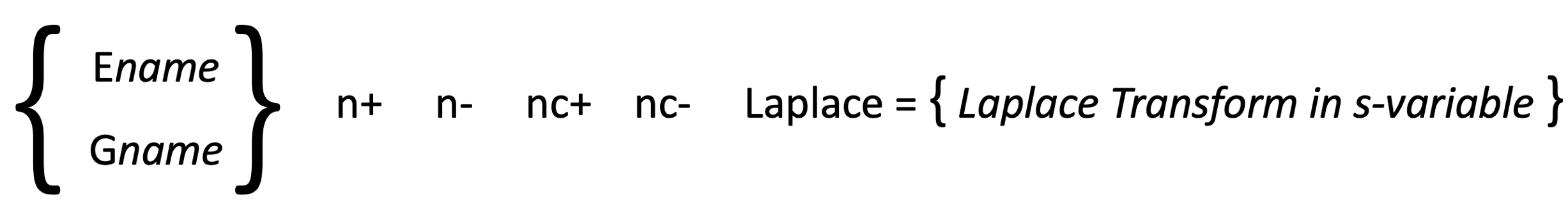
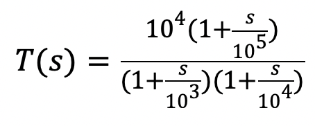
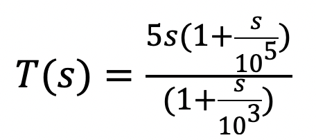
7.1. Use the Laplace transform function of either the voltage-controlled voltage or current source to plot the magnitude and phase response of the following transfer functions:
(i)
![]()
(ii)
(iii)
(iv)
7.2. If in the circuit of Fig. P8.2 is an ideal voltage amplifier of gain 100, use LTSpice to determine AM, wL and wH of this amplifier.
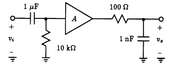
Fig. P8.2
7.3. The low-frequency response of an amplifier is characterized by three poles of frequencies 10 Hz, 3 Hz, and 1 Hz, and three zeros at w=0. With the aid of the Laplace transform function capability of specifying the gain of a dependent source in LTSpice, calculate the lower 3-dB frequency fL and compare this result with the value obtained using: (a) the dominant pole approximation method, and (b) the root-sum-of-squares approximation method.
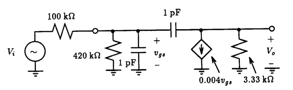
Fig. P8.4
7.4. Fig. P8.4 shows the high-frequency equivalent circuit of a common-source FET amplifier driven by a signal generator having a resistance of 100 kΩ. Using LTSpice, compute the upper 3-dB frequency fH using the method of open-circuit time constants. Compare this result with that obtain directly from the input-output voltage transfer characteristics.
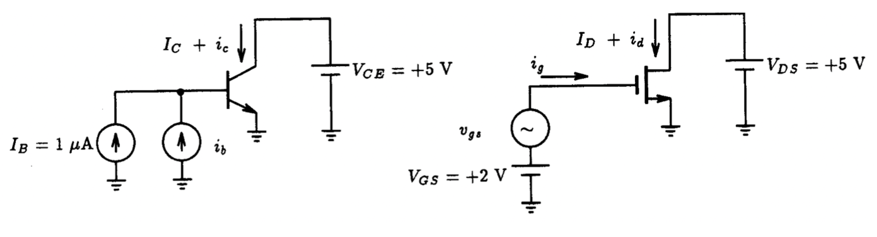
Fig. P8.5. Fig. P8.6
7.5. Using the circuit setup shown in Fig. P8.5, calculate the small-signal current gain ic/ib of the commercial 2N3904 npn transistor using LTSpice. The Spice model parameters for the 2N3904 can be found in the built-in library of LTSpice. What is the corresponding fT of this transistor?
7.6. Using the circuit setup shown in Fig. P8.6, have LTSpice calculate the small-signal current gain id/ig as a function of frequency for an n-channel MOSFET characterized by Vt=1 V, 𝜇n COX=20 𝜇A/V2, L=10 𝜇m, W=30 𝜇m, 𝜆=0.04 V-1, CGSO=1 pF, and CGDO=1 pF. What is the corresponding unity current gain frequency of this transistor?
7.7. A small-signal equivalent circuit of a FET common-source amplifier has Rin=2 MΩ, gm= 4 mA/V, ro=100 kΩ, RD=10 kΩ, Cgs=2 pF, and Cgd= 0.5 pF. The amplifier is fed from a voltage source with an internal resistance of 500 kΩ and is connected to a 10 kΩ load. With the aid of LTSpice, find the following:
(a) The midband voltage gain AM.
(b) The frequency locations of the two poles and zeros by plotting the input-output voltage characteristics as a function of frequency.
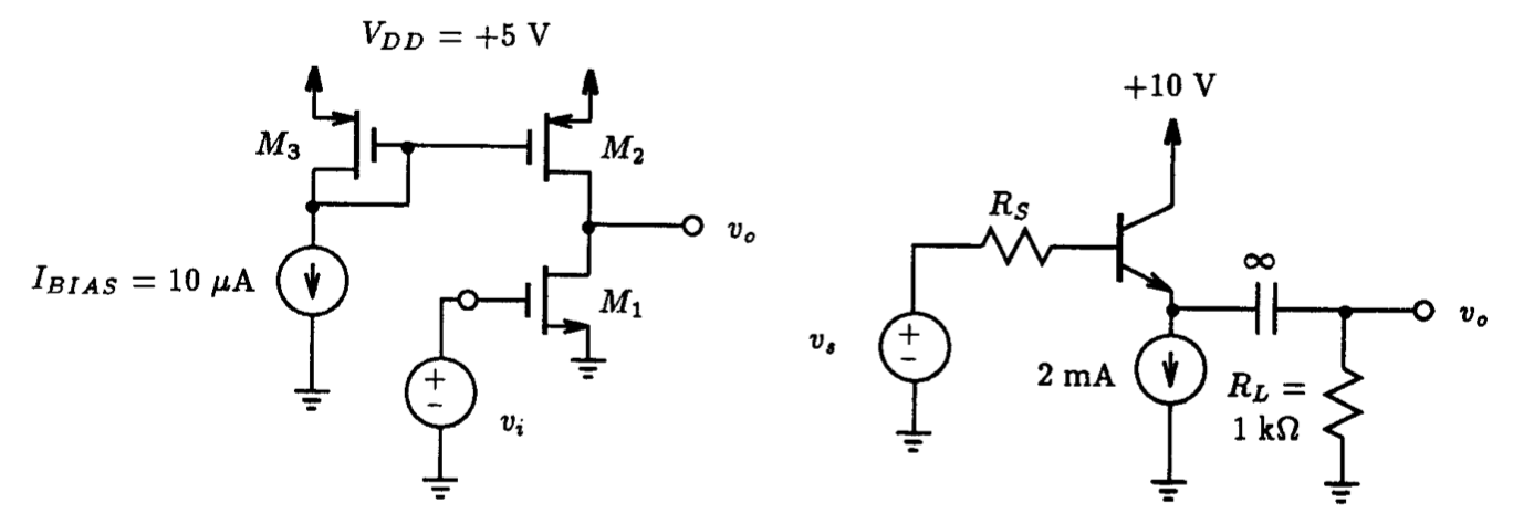
Fig. P8.8. Fig. P8.12
7.8. With the aid of LTSpice, determine the frequency of the pole and zero of the CMOS amplifier shown in Fig. P8.8 in the linear region of the amplifier. For M1, assume the Spice parameters are: Vt=1 V, 𝜇nCOX=20 𝜇A/V2, L=10 𝜇m, W=640 𝜇m, 𝜆=0.02 V-1, CGSO=1 pF, and CGDO=1 pF. For M2 and M3, the Spice parameters are: Vt=-0.8 V, 𝜇pCOX=10 𝜇A/V2, L=10 𝜇m, W=1000 𝜇m, 𝜆=0.02 V-1, CGSO=1 pF, and CGDO=1 pF.
7.9. Consider the common-emitter amplifier of Fig. 8.13(a), with the aid of LTSpice, plot the amplifiers input impedance Zin (magnitude and phase) as seen by the source excluding Rs.
7.10. For the common-emitter amplifier shown in Fig. 8.13(a), if CE is increased to 30 𝜇F, what happens to the bandwidth of this amplifier? Quantify your answer using LTSpice.
7.11. For a 10 kHz, 100 mV sinewave applied to the input of the CC-CE cascade amplifier shown in Fig. 8.13(b), using LTSpice, plot the voltage waveform appearing at the output for at least one complete period of the input signal. Compare these results with those obtained for an input signal increased to 5 V of the same frequency.
7.12. For the emitter-follower shown in Fig. P8.12, with the aid of LTSpice, calculate the midband gain and the upper 3-dB frequency of the amplifier under the following source resistance conditions:
(a) Rs=1 kΩ,
(b) Rs=10 kΩ, and
(c) Rs=100 kΩ.
Assume the transistor is modeled after the commercial 2N3904 npn transistor. In addition, for simulation purposes, replace the infinite-valued decoupling capacitor by a very large value (i.e., 106 pF).
7.13. Plot the waveform appearing at the output of the cascode amplifier shown in Fig. 8.12(b) for a 100-mV input triangular waveform of 1 kHz frequency. Repeat this Spice simulation with the frequency of the input signal increased to 100 kHz. Comment on your results.
7.14. Compare the input-output frequency response behavior of the differential amplifier shown in Fig. 8.18(a) with the transistor modeled after the 2N3904 and 2N2222. Comment on the results. The Spice parameters for the 2N3904 and 2N2222 can be found in the built-in library of LTSpice.
7.15. If the current source used to bias the differential amplifier in Fig. 8.18(a) is assumed to have an output resistance of 200 kΩ, with the aid of LTSpice, compute the CMRR of this amplifier as a function of frequency. Assume that the amplifier is driven differentially. How does these results compare to the CMRR of the CC-CB differential amplifier shown in Fig. 8.18(c) if it is also driven differentially?
7.16. Compute the frequency response behavior of a simple bipolar current mirror circuit. Model each bipolar transistor after the Gennum Corporation integrated npn transistor described in Section 6.4.
7.17. Compute the frequency response behavior of the modified Wilson current mirror and the cascode current mirror circuit of Problem 6.12 of the previous chapter. Model each bipolar transistor after the Gennum Corporation integrated npn transistor described in Section 6.4. Which circuit has the higher frequency response?